
NVIDIA Hopper Architecture
H100 implemented using TSMC’s 4N process customized for NVIDIA with 80 billion transistors,a die size of 814 mm2, and higher frequency design.

NVIDIA H100 Tensor Core GPU Overview
H100 with InfiniBand interconnect delivers up to 30 times the performance of A100.
NVIDIA H100 GPU Key Feature Summary
- New Streaming Multiprocessor
- New fourth-generation Tensor Cores
- New DPX Instructions accelerate Dynamic Programming algorithms by up to 7x over the A100 GPU
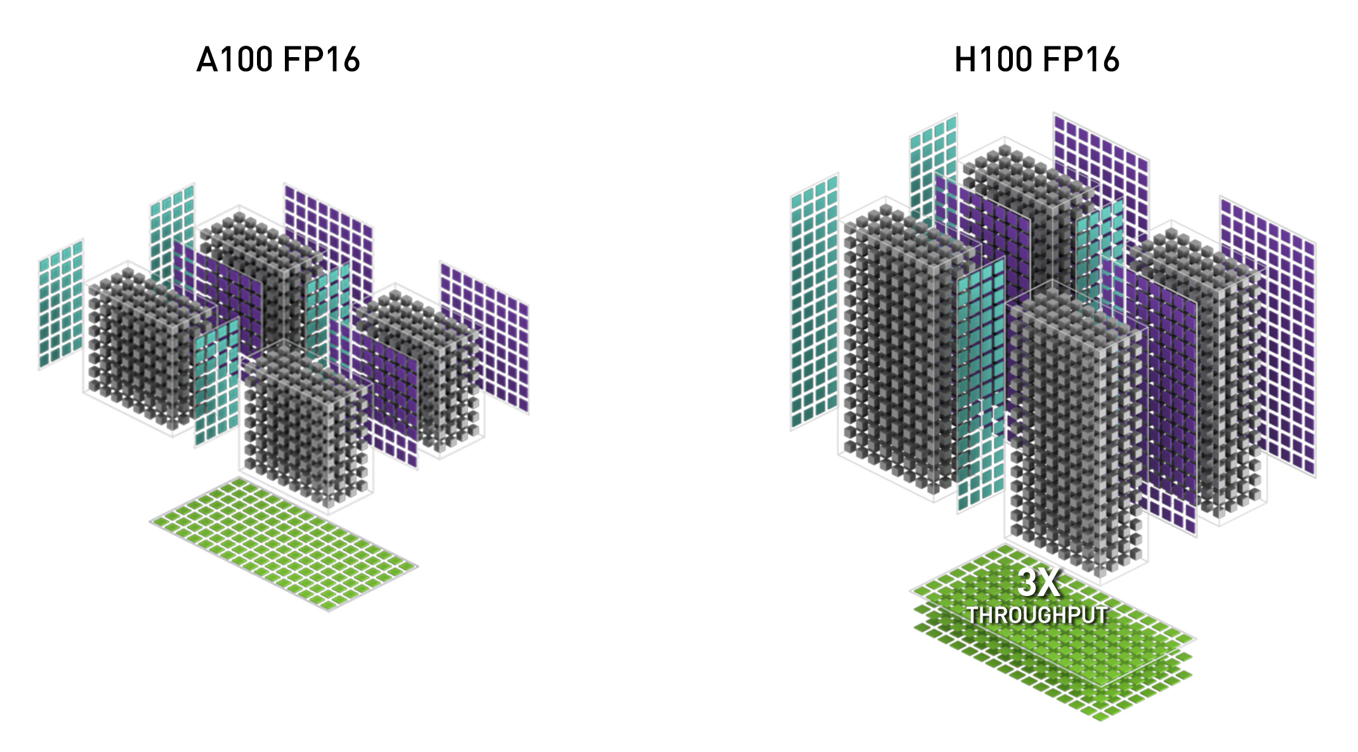
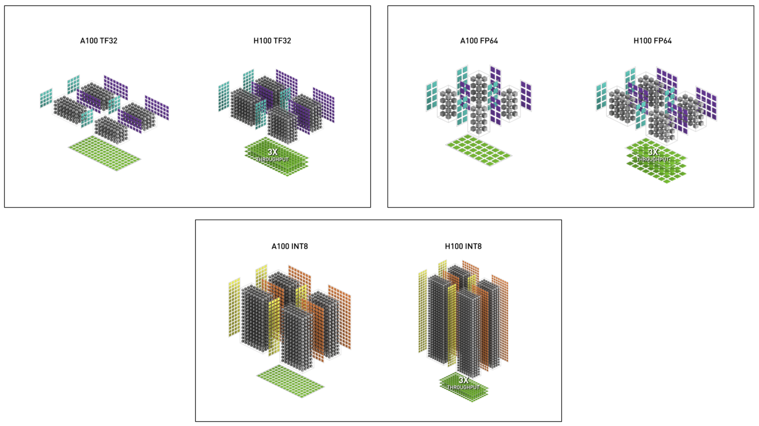
- 3x faster IEEE FP64 and F32
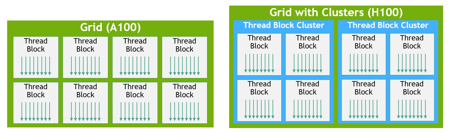
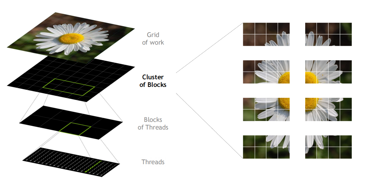
- New Thread Block Cluster feature
- Threads, Thread Blocks, Thread Block Clusters, and Grids
- New Asynchronous Execution features
- Tensor Memory Accelerator (TMA) unit that can transfer large blocks of data very efficiently between global memory and shared memory
- TMA also supports asynchronous copies between Thread Blocks in a Cluster
- New Transformer Engine
- HBM3 memory subsystem
- provides nearly a 2x bandwidth increase over the previous generation
- The H100 SXM5 GPU is the world’s first GPU with HBM3 memory deliveringa class-leading 3 TB/sec of memory bandwidth
- 50 MB L2 cache architecture
- Second-generation Multi-Instance GPU (MIG) technology
- New Confidential Computing support
- Fourth-generation NVIDIA NVLink
- Third-generation NVSwitch
- PCIe Gen 5 provides 128 GB/sec total bandwidth (64 GB/sec in each direction)
NVIDIA H100 GPU Architecture In-Depth
H100 GPU based on Hopper architecture features multiple innovations:
- New 4th Tensor Cores perform faster matrix computation
- New tranformer engine enables H100 to deliver up to 9x faster AI training and up to 30x faster AI inference on large language models
- New NVLink network interconnect enables GPU-to-GPU
| NVIDIA H100 is the first truly asynchronous GPU. H100 extends A100’s global-to-shared asynchronous transfers across all address spaces and adds support for tensor memory access patterns. It enables applications to build end-to-end asynchronous pipelines that move data into and off the chip, completely overlapping and hiding data movement with computation |
Only small number of CUDA threads are now required to manage the full memory bandwidth of H100, most other CUDA threads can be focused on general-purpose computations.
H100 grows the CUDA thread group hierarchy with a new level called the thread block cluster. A cluster is a group of thread blocks that are guaranteed to be concurrently scheduled, and enable efficient cooperation and data sharing for threads across multiple SMs.
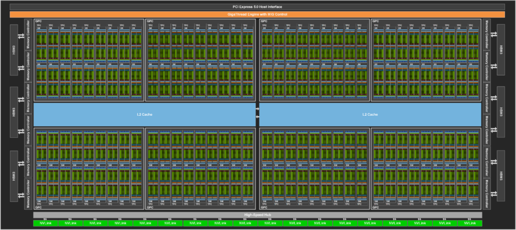
All these new features enable every user and application to use all units of their H100 GPUs fully at all times.The full implementation of the GH100 GPU includes the following units:
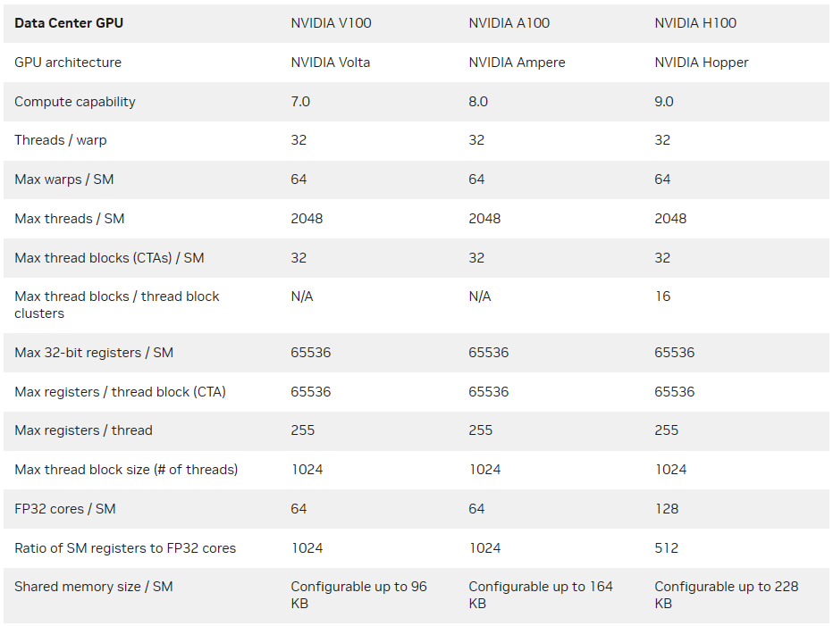
- 8 GPCs, 72 TPCs (9 TPCs/GPC), 2 SMs/TPC, 144 SMs per full GPU
- 128 FP32 CUDA Cores per SM, 18432 FP32 CUDA Cores per full GPU
- 4 fourth-generation Tensor Cores per SM, 576 per full GPU
- 6 HBM3 or HBM2e stacks, 12 512-bit memory controllers
- 60 MB L2 cache
- Fourth-generation NVLink and PCIe Gen 5
Below figure shows a full GH100 GPU which is for AI, HPC, and data analytics, but not graphics processing. Only two TPCs in both the SXM5 and PCIe H100 GPUs are graphics-capable (that is, they can run vertex, geometry, and pixel shaders).
H100 SM Architecture

H100 SM key feature summary
- Fourth-generation tensor Cores deliver 2x the MMA (Matrix Multiply-Accumulate) computational rates of the A100 SM
- New DPX instructions1 accelerate dynamic programming algorithms
- 3x faster IEEE FP64 and FP32 processing rates
- 256 KB of combined shared memory and L1 data cache, 1.33x larger than A100
- asynchronous execution
- New thread block cluster
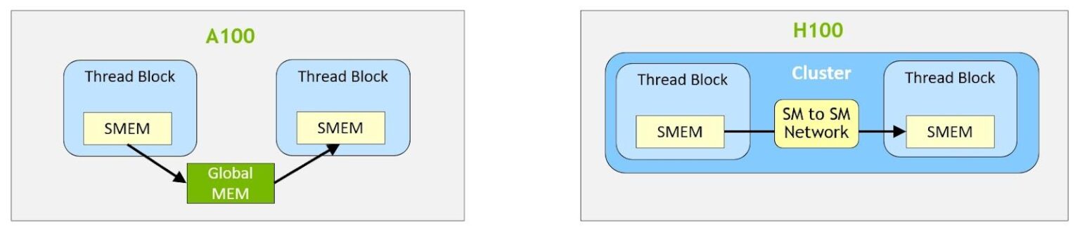
- Distributed shared memory enables direct SM-to-SM communications for loads, stores, and atomics across multiple SM shared memory blocks
H100 Tensor Core architecture
The FP8, FP16, BF16, TF32, FP64, and INT8 MMA data types are supported. The new Tensor Cores also have more efficient data management, saving up to 30% operand delivery power.
NVIDIA Hopper FP8 data format
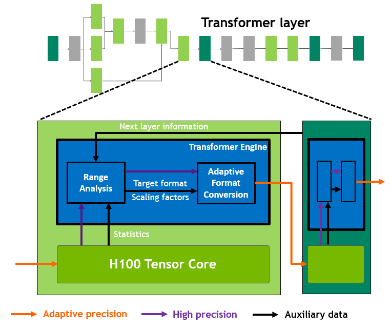
The H100 GPU adds FP8 Tensor Cores to accelerate both AI training and inference.
New DPX instructions for accelerated dynamic programming
These new instructions provide support for advanced fused operands for the inner loop of many DP algorithms.
H100 GPU Hierarchy and Asynchrony Improvements
Thread block clusters
H100 introduces a new thread block cluster architecture that exposes control of locality at a granularity larger than a single thread block on a single SM.
A cluster is a group of thread blocks that are guaranteed to be concurrently scheduled onto a group of SMs, where the goal is to enable efficient cooperation of threads across multiple SMs. The clusters in H100 run concurrently across SMs within a GPC.
Distributed shared memory
With clusters, it is possible for all the threads to directly access other SM’s shared memory with load, store, and atomic operations. This feature is called distributed shared memory (DSMEM) because shared memory virtual address space is logically distributed across all the blocks in the cluster. The dedicated SM-to-SM network for clusters ensures fast, low latency access to remote DSMEM.
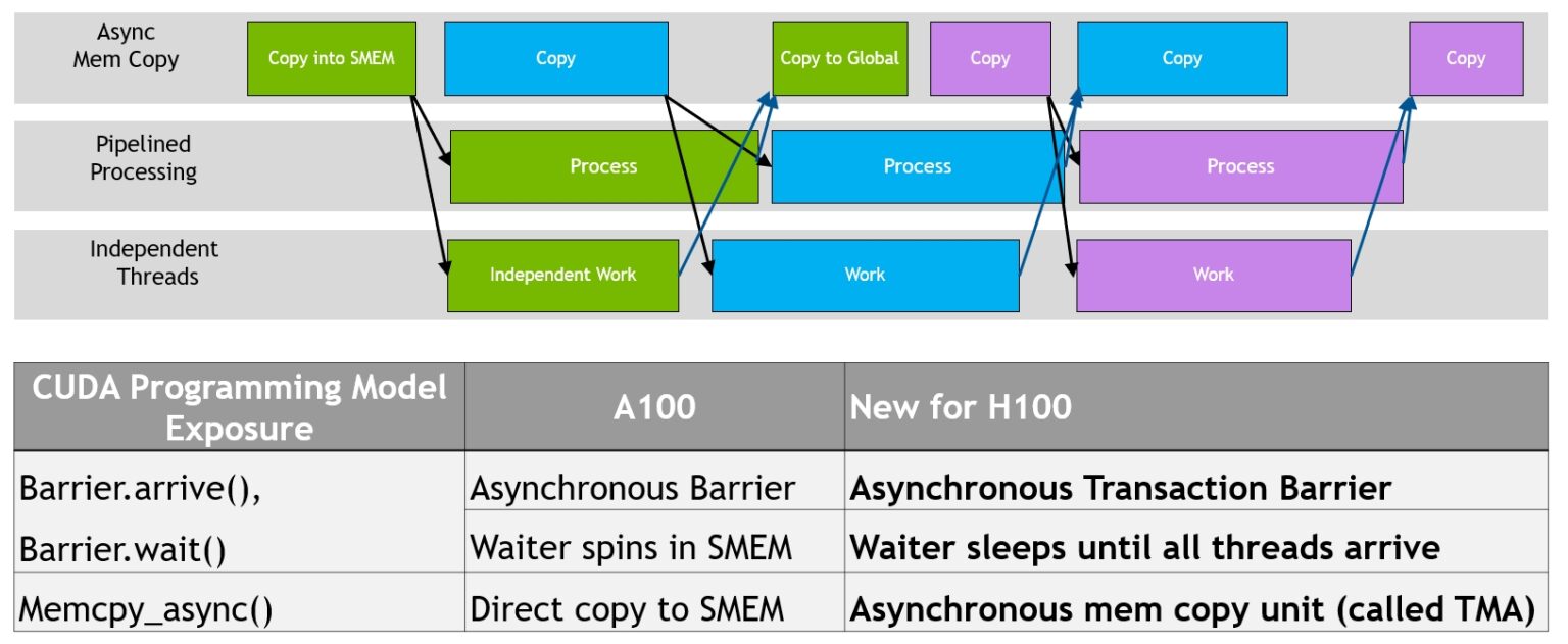
Asynchronous execution
Asynchronous execution capabilities to enable more overlap of data movement, computation, and synchronization.
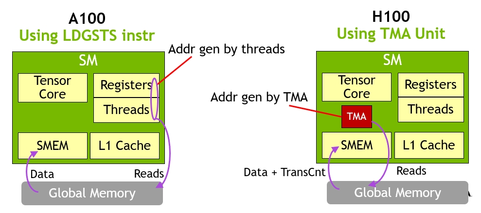
- Tensor Memory Accelerator
- transfer large blocks of data and multidimensional tensors from global memory to shared memory and back again
A key advantage of TMA is that it frees the threads to execute other independent work.
A100的异步memory copy由一个特殊的loadGlobalStoreShared指令执行,所以线程负责产生所有的地址和looping。而在Hopper中,TMA接管所有事情,启动TMA之前,一个线程创建一个copy descriptor,之后所有的地址生成和数据移动都被硬件处理。如下图所示:
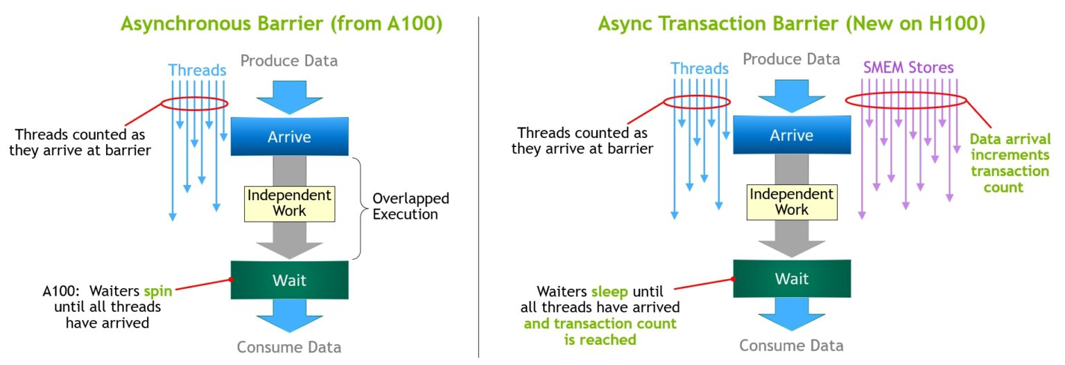
- Asynchronous transaction barrier
- Consider an example where a set of threads are producing data that they all consume after a barrier. Asynchronous barriers split the synchronization process into two steps.
-
- First, threads signal Arrive when they are done producing their portion of the shared data. This Arrive is non-blocking so that the threads are free to execute other independent work.
-
- Eventually, the threads need the data produced by all the other threads. At this point, they do a Wait, which blocks them until every thread has signaled Arrive.
H100 HBM and L2 Cache Memory Architectures
Many memory subsystems exist in a GPU, from the large complement of off-chip DRAM (frame buffer) device memory and varying levels and types of on-chip memories to the register files used in computations in the SM
H100 HBM3 and HBM2e DRAM subsystems
- The H100 SXM5 GPU raises the bar considerably by supporting 80 GB (five stacks) of fast HBM3 memory, delivering over 3 TB/sec of memory bandwidth
- The PCIe H100 provides 80 GB of fast HBM2e with over 2 TB/sec of memory bandwidth
H100 L2 cache
A 50 MB L2 cache in H100 is 1.25x larger than the A100 40 MB L2
Using a partitioned crossbar structure, the L2 cache localizes and caches data for memory accesses from SMs in GPCs directly connected to the partition
Transformer engine
Transformer models are the backbone of language models used widely today from BERT to GPT-3.
H100 includes a new transformer engine that uses software and custom NVIDIA Hopper Tensor Core technology to dramatically accelerate the AI calculations for transformers.
PCIe Gen 5
H100 incorporates a PCI Express Gen 5 x16 lane interface, providing 128 GB/sec total bandwidth (64 GB/sec in each direction)
Summary
The major reason how H100 has higher performance for A100. There are following consideration:
- Clock-for-clock performance per SM