
NVIDIA Pascal Architecture
Tesla P100 is the world’s first GPU architecture to support HBM2 memory.
GP100 is the first NVIDIA GPU to support hardware page faulting, and when combined with new 49-bit (512 TB) virtual addressing, allows transparent migration of data between the full virtual address spaces of both the GPU and CPU.
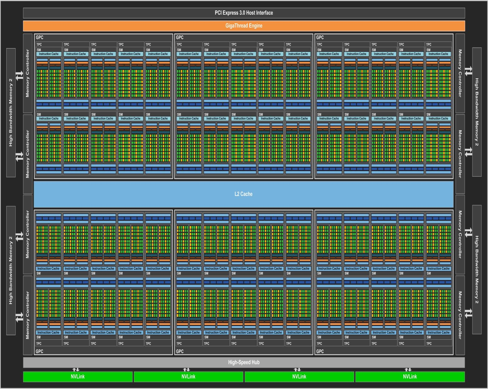
GP100 GPU Hardware Architecture In-Depth
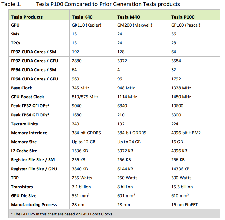
A full GP100 consists of six GPCs, 60 Pascal SMs, 30 TPCs (each including two SMs), and eight 512-bit memory controllers (4096 bits total). Each GPC inside GP100 has ten SMs. Each SM has 64 CUDA Cores and four texture units. With 60 SMs, GP100 has a total of 3840 single precision CUDA Cores and 240 texture units. Each memory controller is attached to 512 KB of L2 cache, and each HBM2 DRAM stack is controlled by a pair of memory controllers. The full GPU includes a total of 4096 KB of L2 cache.
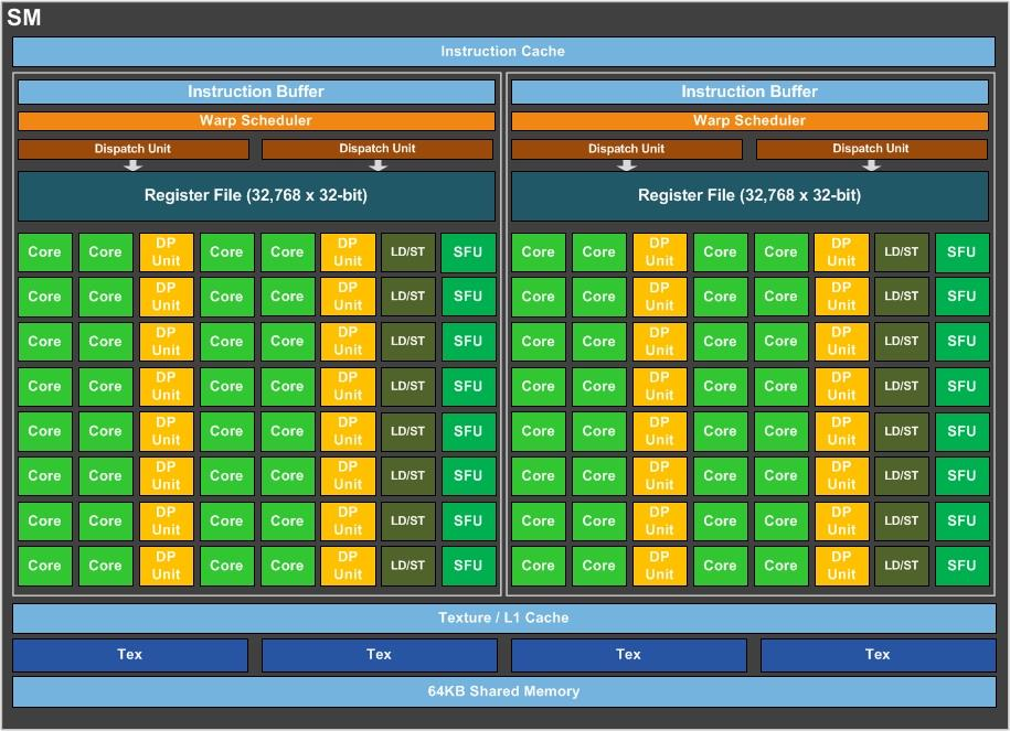
Pascal Streaming Multiprocessor
The GP100 SM is partitioned into two processing blocks, each having 32 single-precision CUDA Cores, an instruction buffer, a warp cheduler, and two dispatch units.
相比Maxwell的SM,Pascal的cuda核数量只有其一半,但保留了相同大小的寄存器文件size. 但是Pascal的SM数量增加了,也就意味相比前一代能支持更多的线程,warp和线程块
每个SM有32 double precision(FP64)CUDA Cores,数量是FP32 single precision CUDA Cores的一半。一个全GP100 GPU有1920 FP64 CUDA Cores。GP100支持full IEEE 754-2008兼容单精度和双精度,包括支持Fused Multiply-Add(FMA)操作。所以在计算算力的时候,每个core的一个clock内可以执行2个操作,一个乘法和一个加法。
Each warp scheduler (one per processing block) is capable of dispatching two warp instructions per clock.
Support for FP16 Arithmetic Speeds Up Deep Learning
Deep learning is one of the fastest growing fields of computing.
Better Atomics
Atomic memory operations are important in parallel programming, allowing concurrent threads to correctly perform read-modify-write operations on shared data structures.
L1/L2 Cache Changes in GP100
The GP100 SM has its own dedicated pool of shared memory (64 KB/SM) and an L1 cache that can also serve as a texture cache depending on workload. The unified L1/texture cache acts as a coalescing buffer for memory accesses, gathering up the data requested by the threads of a warp prior to delivery of that data to the warp.
GP100 features a unified 4096 KB L2 cache that provides efficient, high speed data sharing across the GPU.
NVLink High Speed Interconnect
NVLink is NVIDIA’s new high-speed interconnect technology for GPU-accelerated computing. 用NVLink连接的GPU,程序能直接运行在其他GPU的memory,跟运行在local memory上一样,并且memory operation能保持正确性(例如提供atomic操作的支持)
Unified Memory
Unified Memory History
- The NVIDIA Fermi GPU architecture, introduced in 2009, implemented a unified GPU address space spanning the three main GPU memory spaces (thread private local memory, thread block shared memory, and global memory).
- In 2011, CUDA 4 introduced Unified Virtual Addressing (UVA) to provide a single virtual memory address space for both CPU and GPU memory
- CUDA 6 introduced Unified Memory, which creates a pool of managed memory that is shared between the CPU and GPU, bridging the CPU-GPU divide. Managed memory is accessible to both the CPU and GPU using a single pointer.
Pascal GP100 Unified Memory
Two main hardware features enable these improvements: support for large address spaces and page faulting capability
GP100 extends GPU addressing capabilities to enable 49-bit virtual addressing. This is large enough to cover the 48-bit virtual address spaces of modern CPUs, as well as the GPU’s own memory.
Compute Preemption
The new Pascal GP100 Compute Preemption feature allows compute tasks running on the GPU to be interrupted at instruction-level granularity, and their context swapped to GPU DRAM.