NVIDIA Tesla Architecture
NVIDIA’s Tesla architecture, introduced in November 2006 in the GeForce 8800 GPU, unifies the vertex and pixel processors and extends them, enabling high-performance parallel computing application written in the C-language using the Compute Unified Device Architecture(CUDA) parallel programmig model and development tools.
The first GPU was the GeForce 256, introduced in 1999. In 2001, the GeForce 3 introduced the first programmable vertex processor executing vertex shaders. In 2002, the Radeon 9700 introduced a programmable 24-bit floating-point pixel-fragment processor. In 2005, The XBox 360 introduced an early unified GPU, allowing vertices and pixels to execute on the same processor.
Tesla unified graphics and computing GPU architecture
A primary design objective for Tesla was to execute vertex and pixel-fragment shader programs on the same unified processor architecture.
Tesla architecture is based on a scalable processor array. The below figure shows a block diagram of GeForce 8800 with 128 streamping-processor(SP) cores.

The input assembler collects geometric primitive(points, lines, triangles) and fetches associated vertex input attribute data. It has peak rates of one primitive per clock and eight scalar attributes per clock at the GPU core clock, which is typically 600 MHz.
Streaming Processor Array
Each TPC in the SPA roughly corresponds to a quad-pixel unit in previous architectures. Each SP core contains a scalar multiply-add(MAD) unit, giving the SM eight MAD unit.
Texture/Processor Cluster
Each TPC contains a geometry controller, an SM Controller(SMC), two streaming multiprocessors(SMs), and a texture unit.
Streaming Multiprocessor
The SM is a unified graphics and computing multiprocessor that executes vertex, geometry, and pixel-fragment shader programs and parallel computing programs.
SM consists of eight streaming processor(SP) cores, two special function units(SFU), a multithreaded instruction fetch and issue unit(MT Issue), an instruction cache, a read-only constant cache, and a 16-Kbyte read/write shared memory.
Each SFU also contains four floating-point multipliers.
To efficiently execute hundreds of threads in parallel while running several different programs, the SM is hardware multithreaded. It manages and executes up to 768 concurrent threads in hardware with zero scheduling overhead.
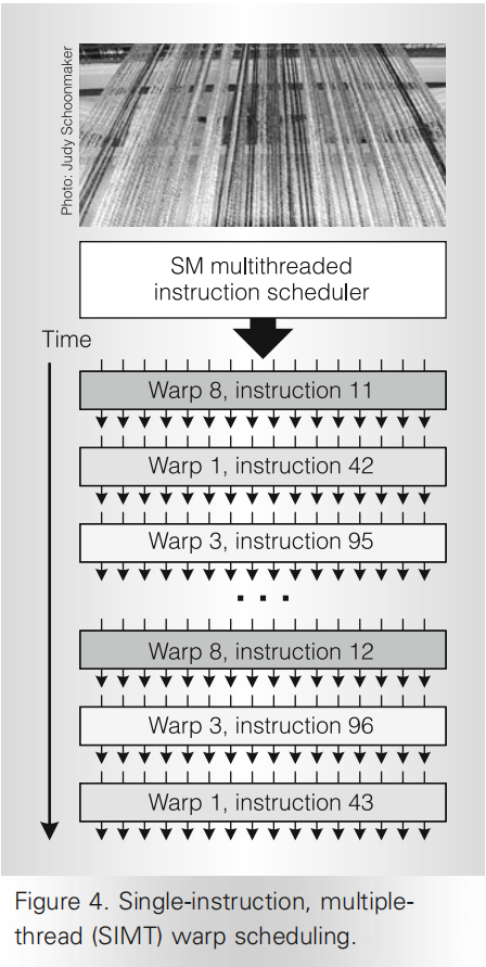
- SIMT
- Single-instruction, multiple-thread
The SM’s SIMT multithreaded instruction unit creates, manages, schedules, and executes threads in groups of 32 parallel threads called warps.
Each SM manages a pool of 24 warps, with a total of 768 threads. At each instruction issue time, the SIMT multithreaded instruction unit selects a warp that is ready to execute and issues the next instruction to that warp’s active threads.
The basic unit of pixel-fragment shader processing is the 2 x 2 pixel quad. The SM controller groups eight pixel quads into a warp of 32 threads. It similarly groups vertices and primitives into warps and packs 32 computing threads into a warp.
- SIMT warp scheduling
- A scoreboard qualified each warp for issue each cycle. This instruction scheduler prioritizes all ready warps and selects the one with highest priority for issue. Prioritization considers warp type, instruction type, and “fairness” to all warps executing in the SM.
- Streaming Processor
- The SP core is the primary thread processor in the SM. It performs the fundamental floating-point operations, including add, multiply, and multiply-add. It also implements a wide variety of integer, comparison, and coversion operations. The unit is fully pipelined, and latency is optimized to balance delay and area.
SM负责调度和分发指令,但SP内有完整的流水线,负责执行指令
- Texture unit
- The texture unit processes one group of four threads(vertex, geometry, pixel, or compute) per cycle.
- Rasterization
- The SMC assembles surviving pixels into warps to be processed by a SM running the current pixel shader.
- Raster Operation Processor
- Each ROP is paired with a specific memory partition. The TPCs feed data to the ROPs via an interconnection network.
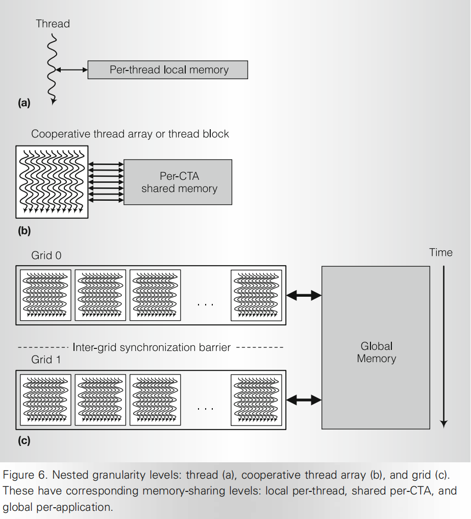
- Cooperative Thread Array or thread block
- Tesla computing architecture introduces the cooperative thread array(CTA), called a thread block in CUDA terminology. Each SM executes up to eight CTAs concurrently, depending on CTA resource demands. When an SM has sufficient available resources, the SMC creates teh CTA and assigns TID numbers to each thread. The SM executes the CTA threads concurrently as SIMT warps of 32 parallel threads. A CUDA thread block is a GPU CTA.
-
-
- thread computes result elements selected by its TID
-
- CTA computes result blocks selected by its CTA ID
-
- grid computes many result blocks, and sequential grids compute sequentailly dependent application steps
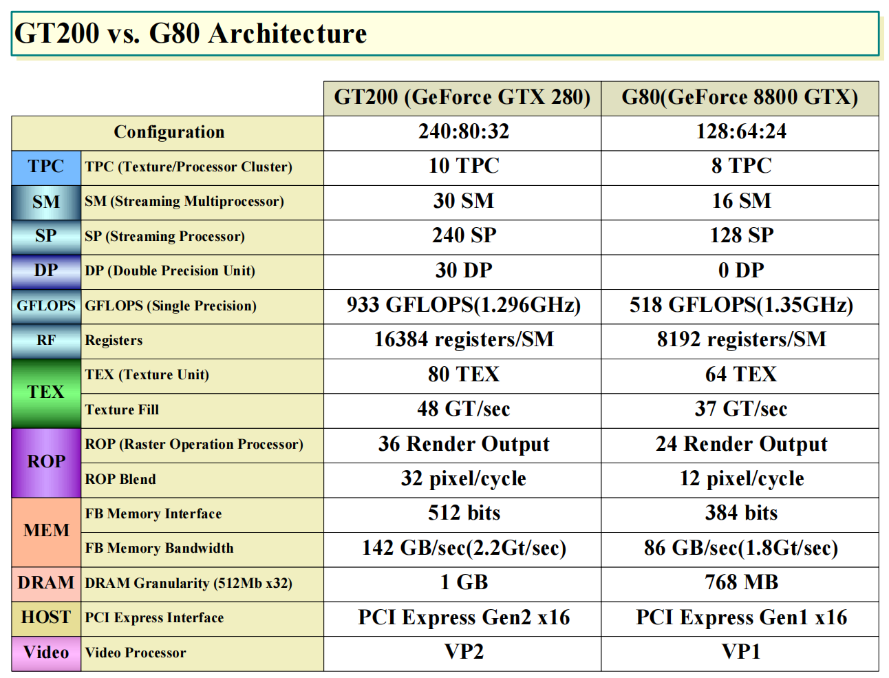
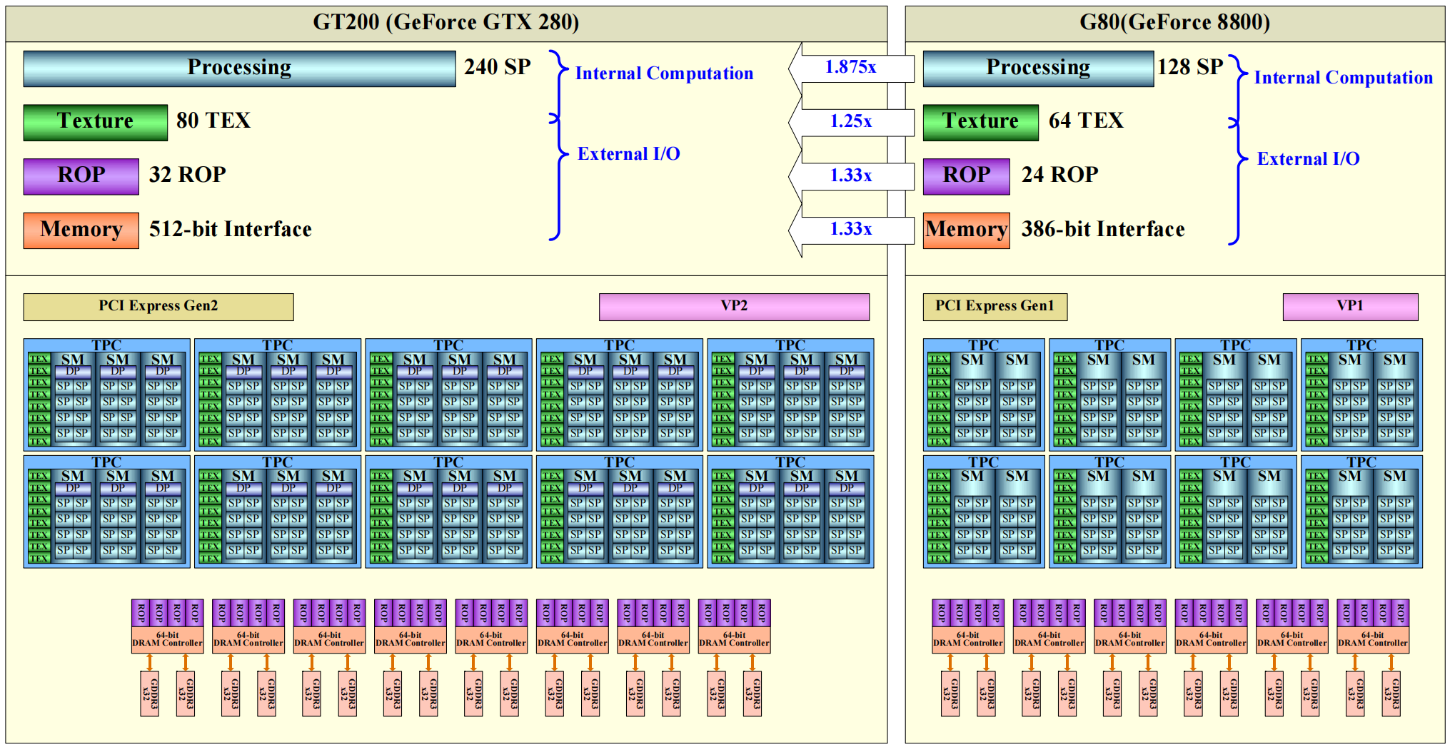
Tesla 2.0 architecture
NVIDIA’s GT200B GPU uses the Tesla 2.0 architecture and is made using a 55 nm production process at TSMC. With a die size of 470 mm² and a transistor count of 1,400 million it is a very big chip. GT200B supports DirectX 11.1 (Feature Level 10_0). For GPU compute applications, OpenCL version 1.1 and CUDA 1.3 can be used. It features 240 shading units, 80 texture mapping units and 32 ROPs.