
NVIDIA Ampere Architecture
Introducing the NVIDIA A100 Tensor Core GPU
Fabricated on the TSMC 7nm N7 manufacturing process, the NVIDIA Ampere architecture-based GA100 GPU that powers A100 includes 54.2 billion transistors with a die size of 826 mm2.
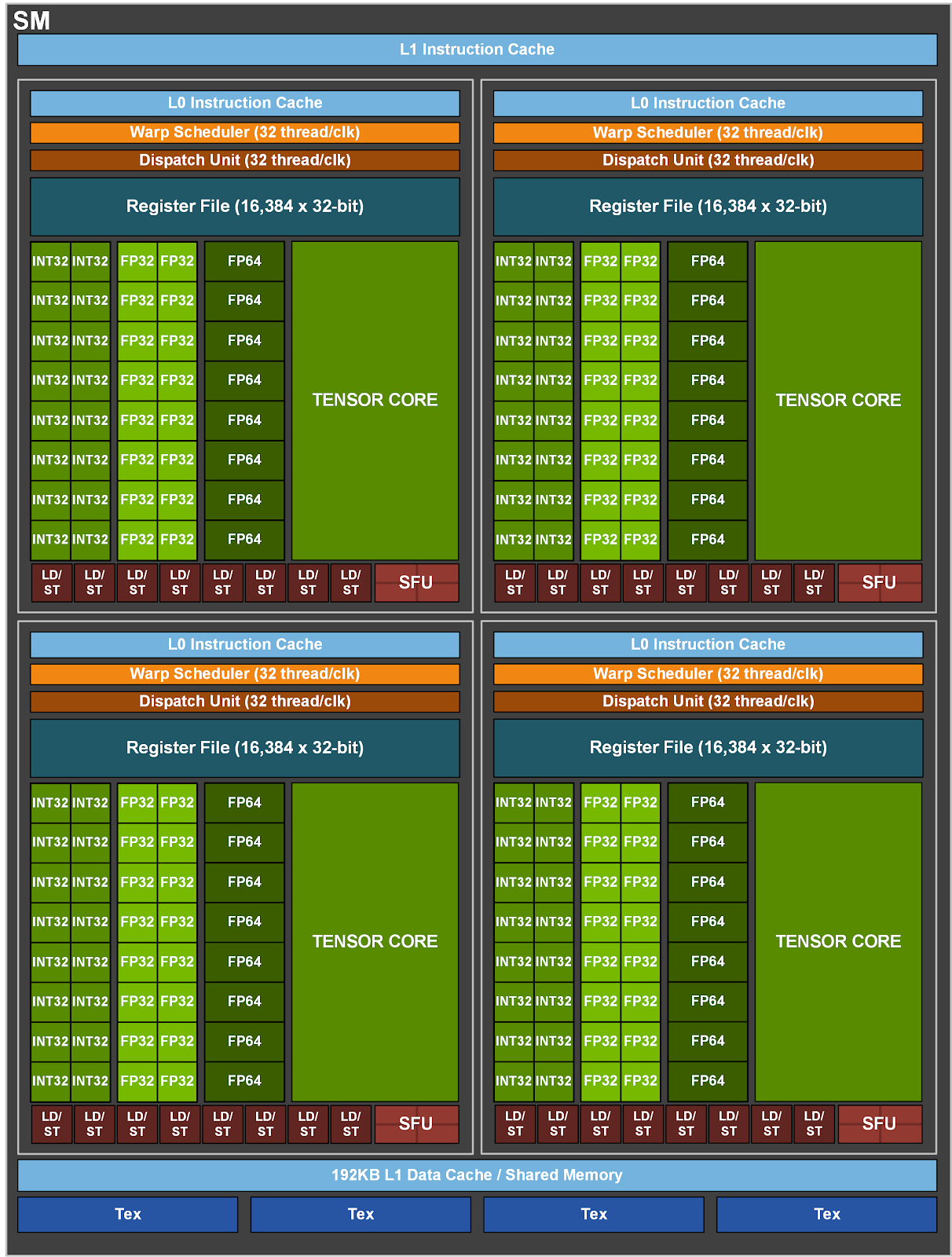
A100 GPU Streaming Multiprocessor
The larger and faster L1 cache and shared memory unit in A100 provides 1.5x the aggregate capacity per SM compared to V100 (192 KB vs. 128 KB per SM)
40 GB HBM2 and 40 MB L2 cache
To feed its massive computational throughput, the NVIDIA A100 GPU has 40 GB of high-speed HBM2 memory with a class-leading 1555 GB/sec of memory bandwidth—a 73% increase compared to Tesla V100. In addition, the A100 GPU has significantly more on-chip memory including a 40 MB Level 2 (L2) cache—nearly 7x larger than V100—to maximize compute performance.
A100 L2 cache provides 2.3x the L2 cache read bandwidth of V100.
Third-generation NVIDIA NVLink
Third-generation NVLink has a data rate of 50 Gbit/sec per signal pair, nearly doubling the 25.78 Gbits/sec rate in V100. The total number of links is increased to 12 in A100, vs. 6 in V100, yielding 600 GB/sec total bandwidth vs. 300 GB/sec for V100.
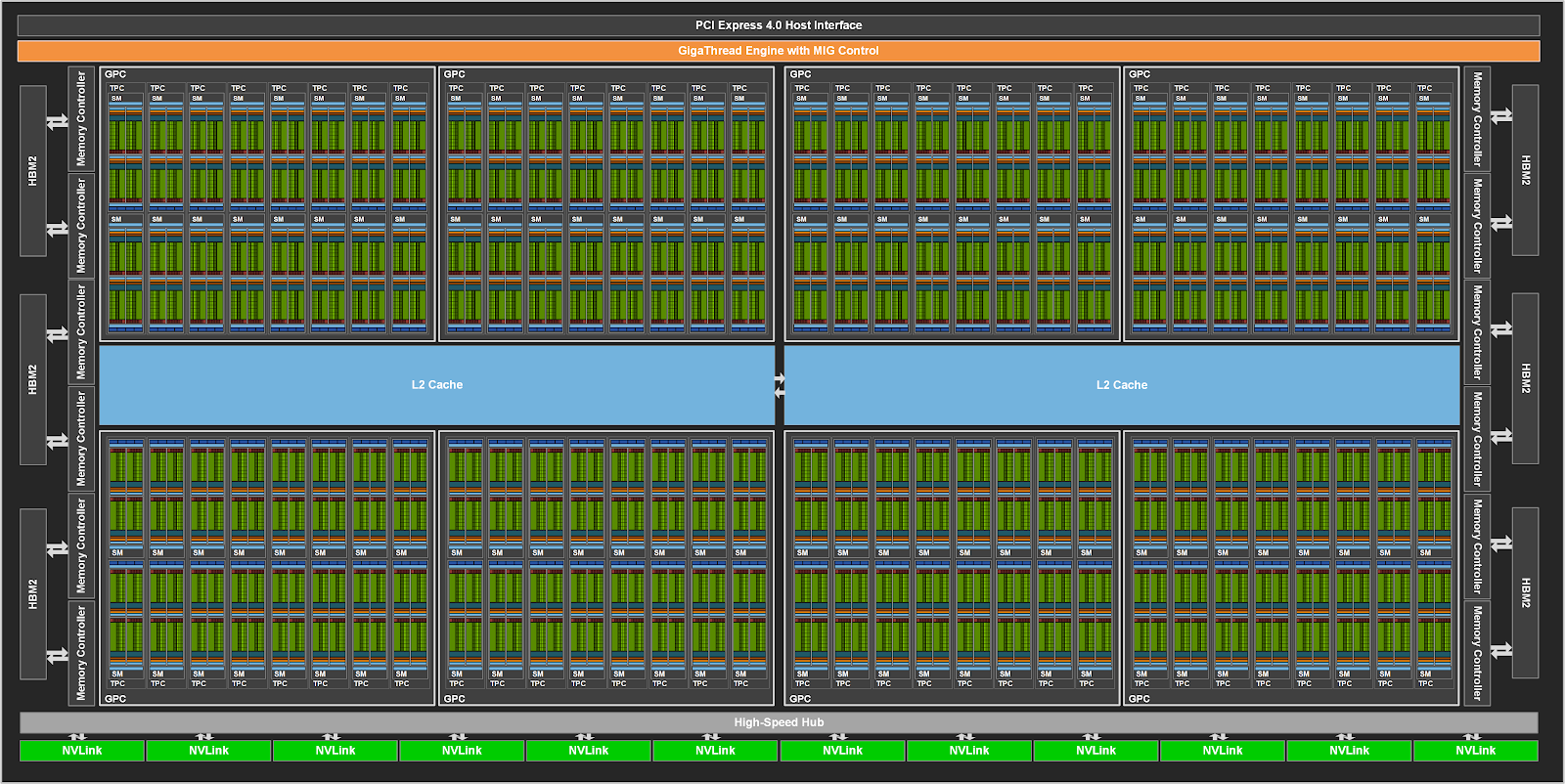
A100 GPU hardware architecture
The NVIDIA GA100 GPU is composed of multiple GPU processing clusters (GPCs), texture processing clusters (TPCs), streaming multiprocessors (SMs), and HBM2 memory controllers.
The full implementation of the GA100 GPU includes the following units:
- 8 GPCs, 8 TPCs/GPC, 2 SMs/TPC, 16 SMs/GPC, 128 SMs per full GPU
- 64 FP32 CUDA Cores/SM, 8192 FP32 CUDA Cores per full GPU
- 4 third-generation Tensor Cores/SM, 512 third-generation Tensor Cores per full GPU
- 6 HBM2 stacks, 12 512-bit memory controllers
A100 SM architecture
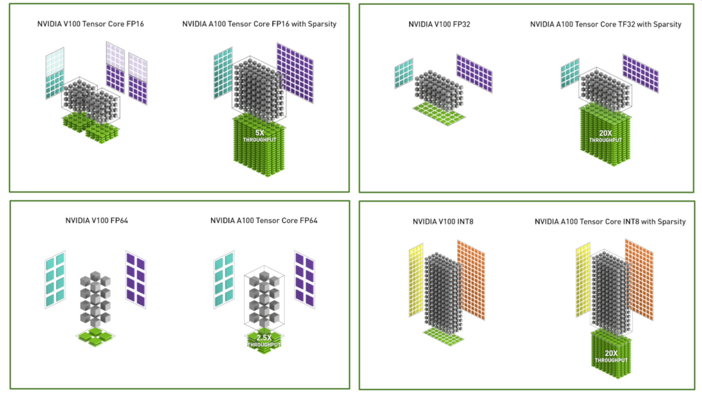
The A100 SM includes new third-generation Tensor Cores that each perform 256 FP16/FP32 FMA operations per clock. A100 has four Tensor Cores per SM, which together deliver 1024 dense FP16/FP32 FMA operations per clock.
- Third-generation Tensor Cores:
- Acceleration for all data types, including FP16, BF16, TF32, FP64, INT8, INT4, and Binary
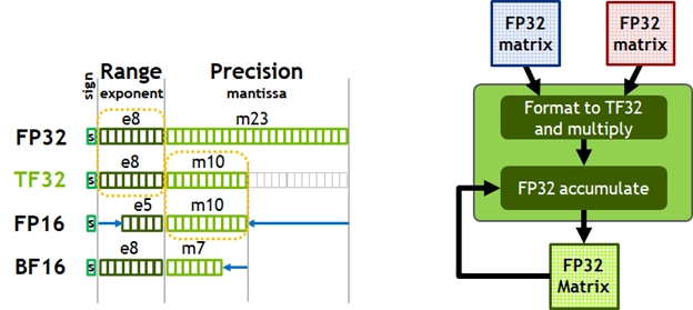
- TF32 Tensor Core operations in A100 provide an easy path to accelerate FP32 input/output data in DL frameworks and HPC, running 10x faster than V100 FP32 FMA operations
- FP16/FP32 mixed-precision Tensor Core operations deliver unprecedented processing power for DL, running 2.5x faster than V100 Tensor Core operations
- BF16/FP32 mixed-precision Tensor Core operations run at the same rate as FP16/FP32 mixed-precision
- FP64 Tensor Core operations deliver unprecedented double-precision processing power for HPC, running 2.5x faster than V100 FP64 DFMA operations
- INT8 Tensor Core operations with sparsity deliver unprecedented processing power for DL inference, running 20x faster than V100 INT8 operations
- 192 KB of combined shared memory and L1 data cache, 1.5x larger than V100 SM
- New asynchronous copy instruction loads data directly from global memory into shared memory
- New shared-memory-based barrier unit (asynchronous barriers) for use with the new asynchronous copy instruction
- New instructions for L2 cache management and residency controls
Below compares V100 and A100 FP16 Tensor Core operations, and also compares V100 FP32, FP64, and INT8 standard operations to respective A100 TF32, FP64, and INT8 Tensor Core operations. Throughputs are aggregate per GPU, with A100 using sparse Tensor Core operations for FP16, TF32, and INT8.
A100 Tensor Cores accelerate HPC
The new double precision matrix multiply-add instruction on A100 replaces eight DFMA instructions on V100, reducing instruction fetches, scheduling overhead, register reads, datapath power, and shared memory read bandwidth.
Each SM in A100 computes a total of 64 FP64 FMA operations/clock (or 128 FP64 operations/clock), which is twice the throughput of Tesla V100.
A100 introduces fine-grained structured sparsity
Sparse matrix definition
Structure is enforced through a new 2:4 sparse matrix definition that allows two non-zero values in every four-entry vector. A100 supports 2:4 structured sparsity on rows, as shown below.
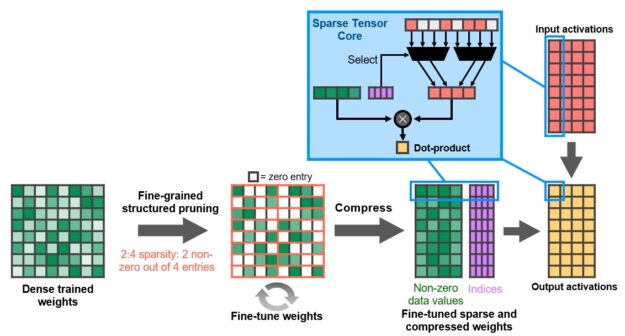
The A100 Tensor Core GPU includes new Sparse Tensor Core instructions that skip the compute on entries with zero values, resulting in a doubling of the Tensor Core compute throughput.
Combined L1 data cache and shared memory
The combined capacity of the L1 data cache and shared memory is 192 KB/SM in A100 vs. 128 KB/SM in V100.
Simultaneous execution of FP32 and INT32 operations
A100 SM also includes separate FP32 and INT32 cores, allowing simultaneous execution of FP32 and INT32 operations at full throughput
A100 HBM2 DRAM subsystem
Tesla P100 was the world’s first GPU architecture to support the high-bandwidth HBM2 memory technology, while Tesla V100 provided a faster, more efficient, and higher capacity HBM2 implementation. A100 raises the bar yet again on HBM2 performance and capacity.
A100 L2 cache
The A100 GPU includes 40 MB of L2 cache, which is 6.7x larger than V100 L2 cache. The L2 cache is divided into two partitions to enable higher bandwidth and lower latency memory access.
Each L2 cache partition is divided into 40 L2 cache slices. Eight 512 KB L2 slices are associated with each memory controller. As mentioned in the MIG section below, an L2 slice group composed of 10 L2 cache slices is included in each GPU slice in a GPU Instance of a MIG configuration. The A100 L2 read bandwidth is 5120 Bytes/clk, compared to V100 L2 cache read bandwidth of 2048 Bytes/clk.
The NVIDIA Ampere architecture provides L2 cache residency controls for the programmer to manage data to keep or evict from the cache (see the CUDA Advances for NVIDIA Ampere Architecture GPUs section below for more details).